 |
Free Web Hosting with PHP, MySQL, Apache, FTP and more. |
 |

|
Free Web Hosting with PHP, MySQL, Apache, FTP and more. |
|

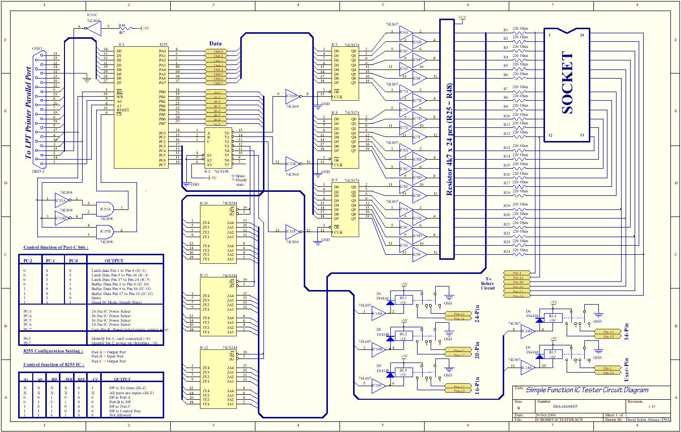
Here is the complete circuit diagram (78.182 Bytes).
The device must used bi-directional LPT
parallel port (because the standard LPT parallel port can not accomodate
the data interchange). All control signals are used to make the combination
of control function for PPI-8255.
More about explanation for this IC type can be seen at another topic, LPT
extender and expander). This IC configured for port-A as output port,
port-B as input port and port-C as output port. Port-A used to send logic
state to IC under test, port-B used to read logic state from IC under test
and port-C used for input decoder to select the enable function of latches
and buffers of IC under test and also to activated the relay power circuits.
Tabel I-1. shows the functional truth table for operational of this PPI-8255
for our purpose.
| A1 | A0 | Reset | Description | |||
| X | X | X | X | 0 | 1 | DP side is tri-state (Hi-Z) |
| X | X | X | X | 1 | X | All ports as input ports (reset) |
| 0 | 0 | 1 | 0 | 0 | 0 | DP side to port-A (write port-A) |
| 0 | 1 | 0 | 1 | 0 | 0 | Port-B to DP side (read port-B) |
| 1 | 0 | 1 | 0 | 0 | 0 | DP side to port-C (write port-C) |
| 1 | 1 | 1 | 0 | 0 | 0 | DP side to port-CW (write port-CW) |
| 1 | 1 | 0 | 1 | 0 | 0 | Not allowed for 8255A-5, but accepted for 82C55 type
(read port-CW) |
As usual, DP port LPT is used for data interchange, PS port LPT used partly
for identify card, and PC port LPT used for controlling the PPI-8255. As
for identify card, like EPROM Programmer
Card application, I used 2-bits for this purpose. But in that card,
PS-7 seems like a redundancy function. Because it is inverting input, so
if the PS-7 bit is not connected/released or broken, the reading also true.
So I make some advanced used for this PS-7 bit. In this IC-Tester card,
this bit used for detecting power-on from the card. If the card is still
connected but the power is off, the program can not continue. Please you
compare this function with both card. All of PC port LPT are used for controlling.
I already selected these bits for our used. PC-5 bit as usual used for
bidirectional enable, PC-3 bit used for WR signal (note that PC-3 is inverting
input), PC-2 bit used for RD signal (this is normal input), PC-1 bit used
for selecting address A1 (note that PC-1 is inverting input) and PC-0 used
for selecting address A0 (this also an inverting input). The others functions,
reset and Chip Select (CS) enable by used the combination of PC-3 and PC-2
bits. The explanation of these functional utilization can be obtain at
LPT
extender and expander topic. Tabel I-2. shows the bits should be apply
to this port for our purpose as needed by tabel I-1.
| DP-7 ~ DP-0 | 8-bit data port | |||||||
| PS-7 (Inv.) | PS-3 | Card Identify | ||||||
| X | 0 | IC-Tester card detect | ||||||
| 1 | X | Power-on detect | ||||||
| PC-7
(Unused) |
PC-6
(Unused) |
PC-5 (Bidirectional Enable) | PC-4
(IRQ Enable) |
PC-3 (Inv.)
Used for |
PC-2
Used for |
PC-1 (Inv.)
Used for A1 |
PC-0 (Inv.)
Used for A0 |
Control port |
| X | X | 0 | 0 | 0 | 1 | X | X | Stand-by mode (Hi-Z) |
| X | X | 0 | 0 | 1 | 0 | X | X | Reset |
| X | X | 0 | 0 | 1 | 1 | 1 | 1 | Writing port-A |
| X | X | 1 | 0 | 0 | 0 | 1 | 0 | Reading port-B |
| X | X | 0 | 0 | 1 | 1 | 0 | 1 | Writing port-C |
| X | X | 0 | 0 | 1 | 1 | 0 | 0 | Writing port-CW |
Port
PC PPI-8255 (for not to be confused between PC port LPT and PC port PPI-8255,
we used the state, PC port is for LPT port and C port for PPI-8255 for
later used) are used for activated the latches, buffers and relays for
IC test power. 3-bits lower used for binary decoder inputs. So we have
8-state from this 3-bits, 3 are used for latches enable, 3 for buffers
enable and 1 for steady-state condition and 1 still spare/unused. Steady
state condition used when there are no action or needs when changing state.
The rest 5-bits of C port used for enable IC test power. Here I only selected
5 possible and general combination for IC's power pins, range for 24-pins
to 14-pins IC. Many TTL's and CMOS's power pins are the last pin number
for Vcc and the half pin number for Ground. So for 24-pins IC, ie.pin-12
and pin-24, for 20-pins IC, ie.pin-10 and pin-20, for 16-pins IC, ie.pin-8
and pin-16, for 14-pins IC, ie.pin-7 and pin-14. If we press the ground
pin to pin-12, many connection are omitted. The last preserved for un-common
combination,ie. if the power locate at another pins, but this is only for
IC type less than 24-pins. Vcc locate at pin-24 and ground at pin-1. Connection
must be made by manual (jumper). You can use some kind of clips with pointed
clip. Fig.1-1. shows one of this clip kinds. For 24-pins IC type, we use
nothing of this relay. This also needs manual conection (jumper) to the
power circuit. Tabel I-3. shows the control function of C port bits.
| C-7 | C6 | C-5 | C-4 | C-3 | C-2 | C-1 | C-0 | OUTPUT |
| 0 | 0 | 0 | Enable latch data pin-1 ~ pin-8 | |||||
| 0 | 0 | 1 | Enable latch data pin-9 ~ pin-16 | |||||
| 0 | 1 | 0 | Enable latch data pin-17 ~ pin-24 | |||||
| 0 | 1 | 1 | Enable buffer data pin-1 ~ pin-8 | |||||
| 1 | 0 | 0 | Enable buffer data pin-9 ~ pin-16 | |||||
| 1 | 0 | 1 | Enable buffer data pin-17 ~ pin-24 | |||||
| 1 | 1 | 0 | Spare (unused) | |||||
| 1 | 1 | 1 | Stand-by mode (steady state) | |||||
| 1 | 1 | 1 | 1 | 1 | User 24-pins IC power select | |||
| 1 | 1 | 1 | 1 | 0 | 24-pins IC power select | |||
| 1 | 1 | 1 | 0 | 1 | 20-pins IC power select | |||
| 1 | 1 | 0 | 1 | 1 | 16-pins IC power select | |||
| 1 | 0 | 1 | 1 | 1 | 14-pins IC power select | |||
| 0 | 1 | 1 | 1 | 1 | User-pins IC power select | |||
Here is the PCB artwork looks like (41.845 Bytes).
Note
that the common copper clad of top layer is ground and the common copper
clad of bottom layer is Vcc. Don't forget to test it with ohm tester (bell
check). this copper side both layer must not short circuited. Also Vcc
and ground for any IC must be checked there were connected or not. Its
better if we used many socket for ICs, because if any IC known defect,
it can be easyly replaced with the new one. Many hours must lost here if
you didn't do it well, careful!!! Here also I made PCB
adapter (8.349 Bytes) for 20-pins, 16-pins and 14-pins IC to 24-pins
socket. View of these adapter constructions
are as follow (8.968 Bytes).
TYPE
    LPT_Port       = (LPT_1, LPT_2, LPT_3, No_LPT);
    Mode_PPI       = (Port_A, Port_B, Port_C, Port_CW, Port_Hi_Z, PPI_Rst);
    Dec_Port_C     = (Set_Latch_1, Set_Latch_2, Set_Latch_3,
                      Set_Buffer_1, Set_Buffer_2, Set_Buffer_3,
                      Set_Spare, Steady_State);
    Mode_Port      = (COM_1, COM_2, LPTs);
    Pin_IC         = (Pin_24, Pin_20, Pin_16, Pin_14, User_Pin, Not_Set);

CONST
     Ada_Port      : BOOLEAN = FALSE;
     Ada_Card      : BOOLEAN = FALSE;
     Bi_Direct     : BOOLEAN = FALSE;
     PC_Port       : ARRAY[0..2] OF WORD =
                     ($03F8,$02F8,$0278);   { 'COM1','COM2','LPT1' }
     DP : ARRAY[LPT_Port] OF WORD = ($3BC, $378, $278, $3BC); { Data Port }
     PS : ARRAY[LPT_Port] OF WORD = ($3BD, $379, $279, $3BD); { Status Port }
     PC : ARRAY[LPT_Port] OF WORD = ($3BE, $37A, $27A, $3BE); { Control Port }
     Port_PPI : ARRAY[Mode_PPI] OF WORD = ($000F,     { Port-A PPI as output port}
                                           $0022,     { Port-B PPI as input port}
                                           $000D,     { Port-C PPI as output port}
                                           $000C,     { Port-CW PPI as output port}
                                           $0004,     { Port-Hi-Z PPI }
                                           $0008);    { Reset PPI }
     Set_Mode_PPI  = $0082;                           { Port-A, Port-C = Output }
                                                      { Port-B = Input, Mode = 0 }
     Set_Dec_Port_C : ARRAY[Dec_Port_C] OF BYTE = ($F8,    { Latch 1 Aktif }
                                                   $F9,    { Latch 2 Aktif }
                                                   $FA,    { Latch 3 Aktif }
                                                   $FB,    { Buffer 1 Aktif }
                                                   $FC,    { Buffer 2 Aktif }
                                                   $FD,    { Buffer 3 Aktif }
                                                   $FE,    { Spare Bit }
                                                   $FF);   { Steady State }
     Tegangan_IC   : ARRAY[Pin_IC] OF BYTE = ($F7,    { Vcc=pin-24, Gnd=pin-12 }
                                              $EF,    { Vcc=pin-22, Gnd=pin-12 }
                                              $DF,    { Vcc=pin-20, Gnd=pin-12 }
                                              $BF,    { Vcc=pin-19, Gnd=pin-12 }
                                              $7F,    { Vcc=pin-24, Gnd=pin-1 }
                                              $FF);   { Vcc=none, Gnd=none, external supply }
     Port_A_PPI    = $03;    { Note that Port-A through Port-CW }
     Port_B_PPI    = $02;    { are inverting to PC-0 and PC-1 }
     Port_C_PPI    = $01;
     Port_CW_PPI   = $00;
PROCEDURE Cek_Card;
VAR
   Kode_1, Kode_2, Kode_3 : BYTE;
   Dummy : BYTE;
BEGIN
     Ada_Port := FALSE; Ada_Card := FALSE;Bi_Direct := FALSE;
     IF (Set_Port = LPTs) THEN         { Parallel Port }
     BEGIN
          FOR LPT := LPT_1 TO LPT_3 DO
          BEGIN
               IF (NOT Ada_Port) OR (NOT Ada_Card) THEN
               BEGIN
                    IF PORT[PC[LPT]] <> Set_Dec_Port_C[Steady_State] THEN Ada_Port := TRUE;
                    IF Ada_Port THEN
                    BEGIN
                         PORT[DP[LPT]] := $44;        { Send code byte 'Dummy' }
                         Dummy := PORT[PC[LPT]];
                         PORT[PC[LPT]] := Dummy OR $20;    { Cek bi-directional port }
                         IF PORT[DP[LPT]] <> $44 THEN Bi_Direct := TRUE;
                         PORT[PC[LPT]] := Dummy;
                         IF Bi_Direct THEN
                         BEGIN
                              IF ((PORT[PS[LPT]] AND $88) = $80) THEN Ada_Card := TRUE   { Cek IC-Tester Card }
                              ELSE Ada_Card := FALSE;      { PS_3 = normal, PS_7 = Inverting }
                         END;                              { When open, PS are all in hi-z }
                    END;
               END;
               IF Ada_Port AND Ada_Card THEN     { Normally PS[LPT] = $7F (?) }
               BEGIN
                    Port_DP := DP[LPT];
                    Port_PC := PC[LPT];
                    Port_PS := PS[LPT];
                    IF Bi_Direct THEN Inisialisasi_PPI;
               END;
          END;
     END;
END;

PROCEDURE Inisialisasi_PPI;
BEGIN
     IF Set_Port = LPTs THEN
     BEGIN
          PORT[PC[LPT]] := Port_PPI[PPI_Rst];    { Give a pulse }
          PORT[PC[LPT]] := Port_PPI[PPI_Rst];    { Give a pulse }
          PORT[PC[LPT]] := Port_PPI[Port_Hi_Z]+Port_CW_PPI;
          PORT[DP[LPT]] := Set_Mode_PPI;
          PORT[PC[LPT]] := Port_PPI[Port_CW];    { Give a pulse }
          PORT[PC[LPT]] := Port_PPI[Port_Hi_Z]+Port_CW_PPI;
          PORT[DP[LPT]] := Set_Dec_Port_C[Steady_State];
          PORT[PC[LPT]] := Port_PPI[Port_C];     { Give a pulse }
          PORT[PC[LPT]] := Port_PPI[Port_Hi_Z]+Port_C_PPI;
     END;
     Temp_Port := Set_Port;
END;

PROCEDURE Tulis_Port_A(Datanya : BYTE);
BEGIN
     PORT[DP[LPT]] := Datanya;
     PORT[PC[LPT]] := Port_PPI[Port_A];     { Give a pulse }
     PORT[PC[LPT]] := Port_PPI[Port_Hi_Z]+Port_A_PPI;
END;

PROCEDURE Tulis_Port_C(Datanya : BYTE);
BEGIN
     PORT[DP[LPT]] := Datanya;
     PORT[PC[LPT]] := Port_PPI[Port_C];     { Give a pulse }
     PORT[PC[LPT]] := Port_PPI[Port_Hi_Z]+Port_C_PPI;
END;

FUNCTION Baca_Port_B : BYTE;
VAR
   Temp : BYTE;
BEGIN
     PORT[PC[LPT]] := Port_PPI[Port_B];     { Give a pulse }
     Temp := PORT[DP[LPT]];
     PORT[PC[LPT]] := Port_PPI[Port_Hi_Z]+Port_B_PPI;
     Baca_Port_B := Temp;
END;
|
All
other parts are still the same as the original software. The menu
(10.531 Bytes) a little different, I omitted the choice for "Test chip
once (slow and fast)" and replace it with "Debugging test" for testing
the new created IC library and "Run test IC" for normally test. Also "Test
Chip Repeatedly until Failure" was omitted, because I thought that this
routine was not very useful.
How the comparing algorithm works? It works like this :
After an IC library file has loaded (or created), every inputs send to the IC pin socket, while the outputs are keep high. After the stable condition arised, the IC output under test will change byt itself, in accordance by the device itself (the kind of gate). And then the logic of IC pin socket read back again, and the outputs are compared to the boolean thruth table from IC library file (so the IC library must exactly meet the data book thruth table).
Original editor still have many bugs, I have improved the editor layout (10.603 Bytes) and keys, so it is convenience to use.If the IC has clock, then the clocks are sending pulse (1 high and 1 low) depends on the clock is a rising edge signal or a falling edge signal (+Clock or -Clock). and then the outputs are read back and compared to the IC library file. If the logic outputs are the same as the data, so the IC device passed, on the other way the device failed. That's all.
*** CHIP TESTER DEVICE FILE
#
#
*** PIN COUNT
Constant_PC_1                 ;IC pin Q'ty
Constant_PC_2                 ;Input pin Q'ty
Constant_PC_3                 ;Output pin Q'ty
Constant_PC_4                 ;Clock(+) pin Q'ty
Constant_PC_5                 ;Clock(-) pin Q'ty
Constant_PC_6                 ;Edited pin Q'ty
*** PIN TYPES
Constant_PT_1                 ;Pin 1
Constant_PT_2                 ;Pin 2
    .                         ;Pin 3 through IC pin Q'ty
    .                         ;Pin types are : 1 = input, 2 = Output,
    .                         ;3 = Clock(+), 4 = Clock(-),
    .                         ;5 = Vcc, 6 = Gnd, 7 = Unused
Constant_PT_(Constant_PC_1)   ;Last IC pin
*** TEST DATA
Constant_TD_0                 ;Step check (Max. 255 step)
Constant_TD_11 Constant_TD_12 ... Constant_TD_1(Constant_PC_6)        ;Matrix for Boolean Truth Table
Constant_TD_21 Constant_TD_22 ... Constant_TD_2(Constant_PC_6)
    .
    .
    .
Constant_TD_(Constant_TD_0)1 Constant_TD_(Constant_TD_0)2 Constant_TD_(Constant_TD_0)(Constant_PC_6)
*** END                       ;Compatibility for Paul Stenning IC Data File Format
*** IC COMPATIBLE TYPES
String_CT_1                   ;Reserved for 7 name
String_CT_2                   ;Max. 8 characters
    .
    .
    .
String_CT_7
*** DESCRIPTION
String_D                      ;Max. 60 characters
*** COPYRIGHT
Originated by: Paul Stenning (1993)
Modified by: David Setya Atmaja (1999)
Sample of this file format for old version
type 7400 IC TTL and new version like this.
As mention from his page, all digital type IC can be checked accept that
those incorporating analog techniques, such as monostables and phase locked
loops. Both TTL's or CMOS's types were accepted. All IC's that have its
boolean thruth table can be implemented here. You can create your own library
database (because mine was not complete yet)
(37.979 Bytes) by inputed this boolean thruth table from data books and experiment with
it. This is what we call, "Hope you having fun with electronics !!!!!".
Now you can download my second version of libraries database (73.641 Bytes)
   1. Resistors :

      R1 ~ R24 = 220 Ohm ...................................................... 24 pcs
      R25 ~ R49 = 4k7 ......................................................... 25 pcs
   2. Capasitors :

      C1 ~ C3 = 100 nF (for IC decoupling, used as necessary ) ................ 3 pcs
      C4 = 470 uF/16V (for power input) ....................................... 1 pcs
   3. Semiconductors :

      IC1  = PPI-8255A-5 or equivalent type (Parallel Peripheral Interface) ... 1 pcs
      IC2 = 74LS138 (3 to 8 channel decoder) .................................. 1 pcs
      IC3 ~ IC5 = 74LS374 (Octal latch) ....................................... 3 pcs
      IC6 ~ IC9, IC14 = 74LS07 (Hex buffer) ................................... 5 pcs
      IC10 ~ IC12 = 74LS244 (Octal tri-state bus driver) ...................... 3 pcs
      IC13 = 74LS04(Hex Inverter) ............................................. 1 pcs
      IC15 = 74LS08 (Quad and gates) .......................................... 1 pcs
      D1 ~ D5 = 1N4001 (optional) ............................................. 5 pcs
   4. Others :

      IC socket for IC test (24-pins) or better zif-socket like textool ....... 1 pcs
      Optional IC socket for 40-pins .......................................... 1 pcs
      Optional IC socket for 20-pins .......................................... 6 pcs
      Optional IC socket for 16-pins .......................................... 1 pcs
      Optional IC socket for 14-pins .......................................... 7 pcs
      LPT-Connector, DB-25 socket (female) .................................... 1 pcs
      Miniature relay (PCB type relay) 5V-DC .................................. 5 pcs
      Miniature jack socket for power supply input ............................ 1 pcs
      Optional On/Off switch for power supply input ........................... 1 pcs
      Optional power indicator for power supply input (R = 470 + Red LED) ..... 1 pcs
      Optional parallel cable (male to male) DB-25 ............................ 1 pcs
IC sockets are optional, but I suggest that you better used it, because the prices are not very much, but it can help if some ICs not work normally. Capacitors for decoupling not drawn in the schematic diagram, but implementing in the PCB, use it as necessary, also capasitor for power supply input. On/off switch and power indicator also optional. I used in my prototype for standardize only. For the relay I got the PCB mounted type, so it can be accepted 14-pins IC socket. If this kind of relay used, it's no need to put any diode. For connecting to LPT port, use only cable for parallel connection (printer data switch cable, not for laplink cable or serial transfer cable).
DB-25 (Female) IC socket (40-pins)By doing this we can connect it either to expander card from lpt port or from decoder card. Also it can accept any other card if it doesn't base on 8255-PPI, but requires 3 consecutive port configured as first and third port as output port and second port as input port. The software must be changed to take this optional design. I already compiled the new version and you can download it here. Here is the prototype after modify (6.707 & 22.339 Bytes).pin-1 -------------------- pin-4 (port A-0)
pin-2 -------------------- pin-3 (port A-1)
pin-3 -------------------- pin-2 (port A-2)
pin-4 -------------------- pin-1 (port A-3)
pin-5 -------------------- pin-40 (port A-4)
pin-6 -------------------- pin-39 (port A-5)
pin-7 -------------------- pin-38 (port A-6)
pin-8 -------------------- pin-37 (port A-7)
pin-9 -------------------- pin-18 (port B-0)
pin-10 -------------------- pin-19 (port B-1)
pin-11 -------------------- pin-20 (port B-2)
pin-12 -------------------- pin-21 (port B-3)
pin-13 -------------------- pin-22 (port B-4)
pin-14 -------------------- pin-23 (port B-5)
pin-15 -------------------- pin-24 (port B-6)
pin-16 -------------------- pin-25 (port B-7)
pin-17 -------------------- pin-14 (port C-0)
pin-18 -------------------- pin-15 (port C-1)
pin-19 -------------------- pin-16 (port C-2)
pin-20 -------------------- pin-17 (port C-3)
pin-21 -------------------- pin-13 (port C-4)
pin-22 -------------------- pin-12 (port C-5)
pin-23 -------------------- pin-11 (port C-6)
pin-24 -------------------- pin-10 (port C-7)
pin-25 -------------------- pin-7 (ground)
![]() References
:
References
:
Created on : October 15, 2000.
-
by : David Setya Atmaja
Persons who interest so far :
![]()