Computer Nerd Kev |
Home|About|Projects|Links |
Projects > OctaBeat |
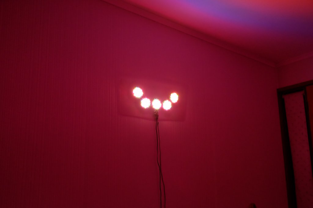
OctaBeat Music Visualiser |
A popular application of SCRs (Silicon Controlled Rectifiers - semiconductors that can be switched on, but not off, by a control signal, suited for driving high-power AC loads) when they were new in the 1970s was to control coloured lights in reaction to different sounds in music by passing the audio through RC filters. Where the filtered audio was of sufficient amplitude to turn on the SCR, it would power a coloured light corresponding to the frequency selected by the filter.
Using op-amps, more accurate filtering and triggering is possible, allowing amplitude and finer features of the audio to be represented in the varied brightness of modern high-brightness LEDs. This forms the basis of Master OctaBeat boards, which can then be connected to Slave boards that feature a microcontroller, and this is used to store the state of the LEDs in a buffer for a configured period of time before repeating it on their own LEDs. This allows a time delay feature to be added to the conventional colour organ effect.

OctaBeat boards connect together on 8pin headers around their perimeter, allowing LED state signals, as well as clock, delay, and audio signals to be shared between all boards in the arrangement. Connection to external power and audio input can be made using add-on boards, such as the Socket and Mic. add-on board for which a schematic is provided below.
OctaBeat kits, bare PCBs, and assembled boards are available from the OmberTech online store, or on Tindie and Ebay.

Both Master and Slave circuitry is shown in this schematic. Note that the output transistors and associated resistors in the Master area are also used for the Slave build. The LEDs on the front of the OctaBeat board are not shown.
The following is extracted from the OctaBeat manual, which can be downloaded at the links above.
The circuit used for the OctaBeat Master boards includes two stages of Resistor-Capacitor filtering, separated by Op-Amps IC1A and IC2A (the gain of which may be adjusted via RV2 and RV3 in order to calibrate the sensitivity) in the high and low frequency detection stages. The output from these filters is fed to Op-Amp comparators IC1B and IC2B which turn on their corresponding colour of LEDs via Q3 and Q9 only when the filtered audio signal voltage is greater than their reference of 4.9V set by the voltage divider R15 and R16.
While conventionally another filter stage is used to detect the mid-range frequencies, here some components are saved by using the filtered input signals for the low and high range comparators. IC1A and IC2A are used in inverting configuration, so their AC output waveforms are opposite in voltage to the input audio signal. By mixing these filtered, inverted, signals with the original input signal, the waveforms that passed through the high or low filters are cancelled out in the signal fed to the Mid comparator, IC1C. The audio signals that do make it through are therefore the ones between the thresholds of the low and high filters - the mid-range frequencies. The mixer is composed of R3, R4, and R5.
The amplification of the non-inverting input amplifier, IC1D, is set by RV1. The audio input is passed through C1, and referenced to a 4.5V virtual ground which is also used by all of the amplifier stages later in the circuit. This virtual ground reference is half of the 9V supply voltage for the Op-Amps, which is regulated from the 12VDC supply by REG1. The voltage divider of R17 and R18 sets the virtual ground reference voltage.
The remaining Op-Amps from the IC2 quad op-amp chip, are used to generate the control signals for the slave boards. IC2C is configured as a square-wave oscillator to produce a clock signal that controls the rate and timing of the slave boards as they sample data. IC2D buffers the delay voltage which is set by a voltage divider formed by R28 and the resistor selected by the DIP switch (R30 - R33), or alternatively by trimpot RV4 if it is selected. Alternatively, J3 can be used to select the input audio signal to be supplied on the Delay line, thereby enabling the microcontroller on slave boards to process the audio using its own ADC. In this case the voltage is reduced using the voltage divider R39 and R40 to below 3.3V so that the microcontroller inputs are protected.
R9 and R10 similarly provide a reference voltage of 2.7V which is used as the maximum voltage level of the Clock and Delay signals. Q10 buffers the clock signal because the positive swing of the Op-Amp oscillator IC2C's output is to its 9V supply.
The signals at the collectors of Q1 to Q3 not only pull Low the base of Q7 to Q9, permitting the LEDs to turn on, but also connect with the output headers via D2 - D4 (shown on the "slave" side of the schematic) to supply the active-low signal read by the salve boards, or directly controlling Q7 to Q9 on "dumb" boards that are connected. R46 - R48 pull these signals high in order to supply enough reverse current through diodes D2 to D4 and into the microcontroller inputs, otherwise the amplified current via Q7 - Q9 is enough to cause a dim glow in the high brightness LEDs.
Slave boards do away with all of the Op-Amps and associated analogue circuitry, while keeping the LED driver transistors Q7 - Q9 which are now driven by a PIC24EP32GP202 microcontroller (16bit, 4KB RAM) via Q4 - Q6. This microcontroller includes an internal RC oscillator which is used as its clock source. The microcontroller samples the LED state inputs (port B) from the stage connected to its header socket on every cycle of the clock signal, writing the three bits of data to RAM. The data that was previously in that RAM location is written to the outputs (port A), and with each pair of three-bit state values (two states are stored per 8bit byte) a pointer variable is incremented so that the next RAM address is used following the next clock cycle. The analogue voltage value read from the Delay signal using the ADC is scaled to set a maximum address value for the LED state data. When this highest address is reached, the process begins again from the starting address. As a result, a buffer of LED state values is created, and written values are only read from it after the program has advanced over the full range of RAM addresses that it spans. The equivalent in digital logic is a massive SISO (Serial-In, Serial-Out) shift register, with thousands of stages.
Brightness control is achieved by sampling the input data fast enough that the width of the short pulses, where the Op-Amp comparators in the Master board go High as the peak of their input waveform exceeds the threshold voltage, is recorded. This is somewhat similar to software PWM (Pulse-Width Modulation), because the volume of the audio increases the time during which the waveform is above the comparator threshold, and therefore the output pulse width, turning the LED on for longer and appearing brighter. Though the actual PWM frequency varies depending on the frequency of the individual sound waveforms.
The input LED state signals are actually active-Low due to the inversion of Q1 - Q3 on the master board, or Q4 - Q6 on the slaves, so they are inverted by the microcontroller before being written to the outputs.
These boards simply connect their LED driver transistors (Q7 - Q9) in parallel with those on the board in the previous stage. They are driven directly by the LED state input signals, and therefore by either Q1 - Q3, or Q4 - Q6 depending on whether the previous stage is a Master or a Slave board.
The LED state signals at the inputs and outputs are joined, so following Dumb stages can also be connected, as well as Slaves, still being driven by the transistors in the previous Master or Slave stage.
By disconnecting the J4 jumper, an external delay voltage input can connected at any of the headers on a connected board, eg. for easier manual adjustment. At a minimum, this can be a potentiometer with the wiper connected to the Delay signal, and the other connections to GND and a voltage safely under 3.3V (2.7V is used in the Master circuit). Connecting a voltage higher than the microcontroller's supply could easily cause damage, though R42 on the Slave board is intended to provide some degree of protection against this by limiting the input current.
The hardware design allows for additional functions by the microcontroller firmware, though these are not currently implemented.
The microcontroller inputs connected to the Clock and Delay signals, which are shared by all connected boards, can be configured in firmware to be used by the internal UART. As such they can be used as a serial bus for communication. This allows adding support for lighting control protocols such as DMX, with an Add-On board connecting one of the input headers in order to provide the required connectors and level conversion.
To aid such digital control of the Slave boards, microcontroller outputs that can be configured for use with the internal hardware PWM module are connected in parallel with the port A connections which are normally used for controlling the LEDs from software.
The two data connections to the ICSP header could also be used with the microcontroller's programmable pull-up/down function in order to provide configuration inputs using jumpers. For example, the presence of a jumper between pins 3 and 4 could be detected, and used to cause a modified firmware to enter an alternative operating mode. With the two inputs available, four individual settings can potentially be configured.
The ADC could be used for digital processing of the audio signal as an alternative to the analogue filtering used by the Master board.
Source code for the PIC24 microcontroller firmware is available from the OctaBeat webpage and can be compiled with the free version of the XC16 C compiler available from the Microchip website.
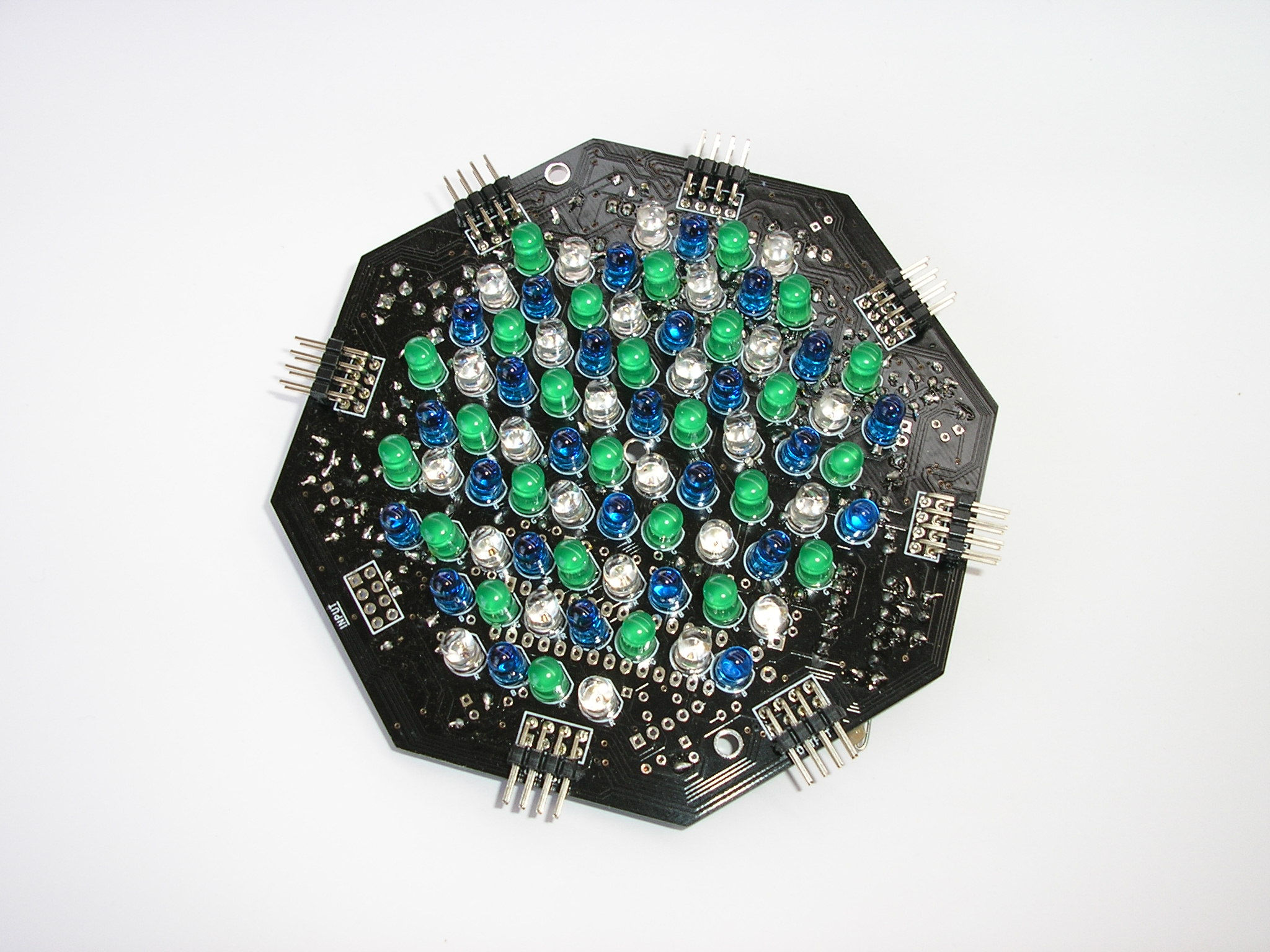
The LED brightness is determined by current-limiting resistors R50 - R62. In the standard kits from OmberTech, high brightness LEDs are used so that the total current required is kept reasonable while still producing a bright display.
If LEDs of different brightness ratings are used, find the current/LED at which they produce a suitable brightness for this application without excessive total current draw.
The LEDs on the board are connected in parallel within thirteen banks, each current limited by a corresponding resistor R50 - R62. In order to allow for an efficient PCB layout the number of LEDs per bank varies between four and nine. The following table shows the banks associated with each current-limiting resistor:
| Resistor | No. LEDs | Range |
|---|---|---|
| R50 | 4 | HIGH |
| R51 | 6 | MID |
| R52 | 8 | LOW |
| R53 | 5 | HIGH |
| R54 | 6 | MID |
| R55 | 6 | MID |
| R56 | 5 | LOW |
| R57 | 6 | HIGH |
| R58 | 7 | HIGH |
| R59 | 5 | HIGH |
| R60 | 9 | MID |
| R61 | 5 | LOW |
| R62 | 8 | LOW |
Take the current required per LED determined earlier and multiply it by the number of LEDs in each bank for that colour (range) to get the total current required for that bank. Subtract the voltage drop over the LED (usually around 2V) from the 12V supply, and divide that voltage by the total current to get the resistance value required for each LED bank.
Adjusting the input amplifier via RV1 also allows for some minor adjustment of overall brightness after the board has been assembled.