
Computer Nerd Kev |
Home|About|Projects|Links |
Projects > Logic Visualiser |
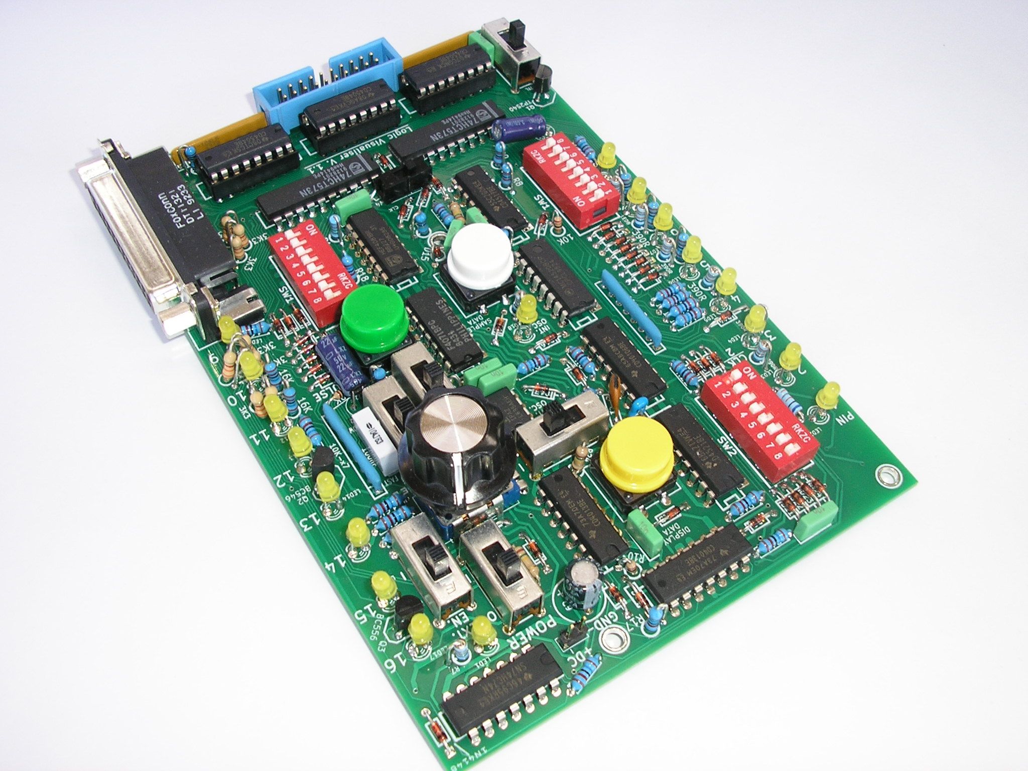
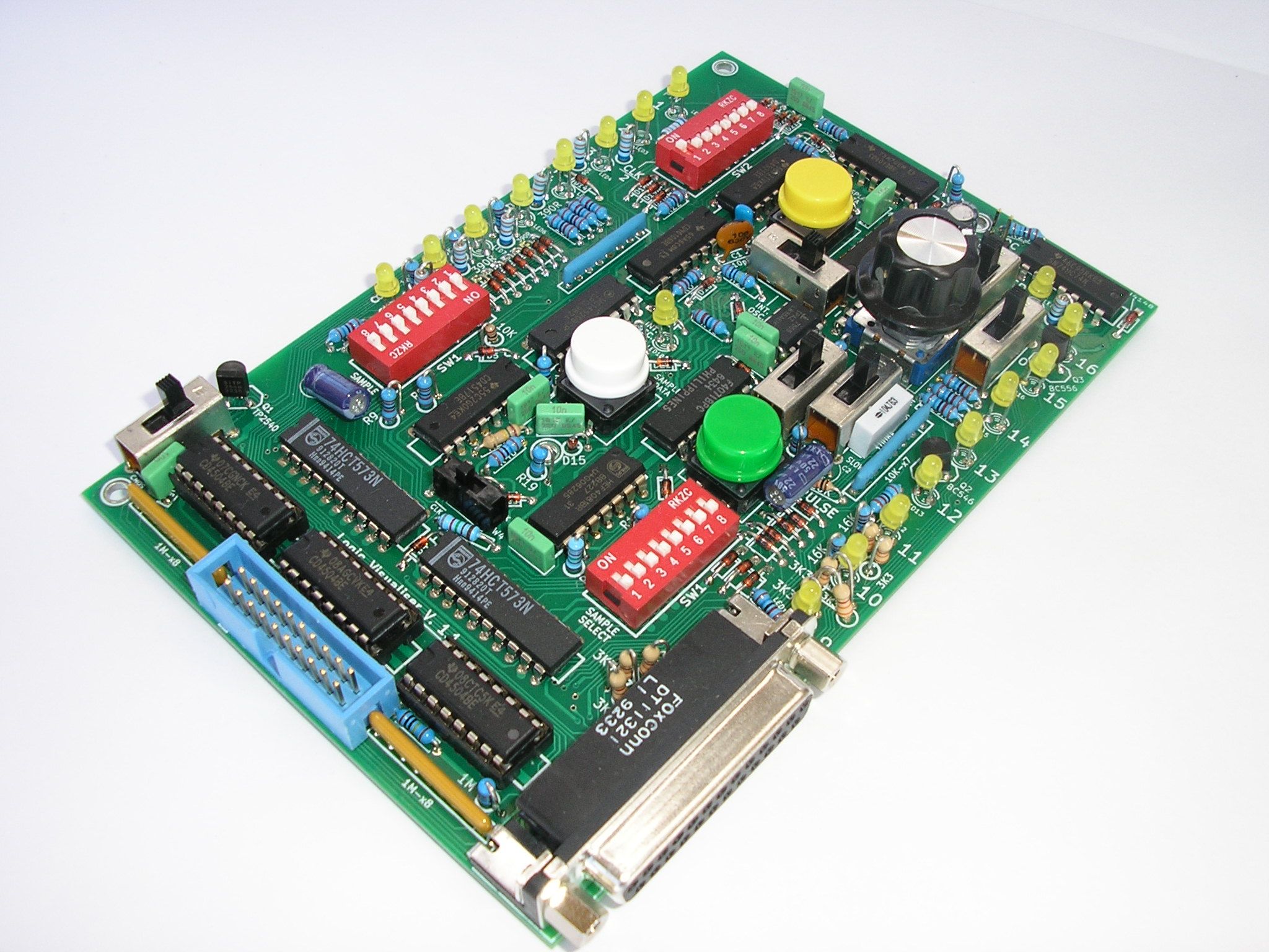
The Logic Visualiser |
This page hosts the documentation for my Logic Visualiser project, available in kit form from the OmberTech web store, or on Tindie. The following is from the introduction of the Logic Visualiser booklet, available for download below.
The Logic Visualiser is designed as a simpler, smaller, (to say nothing of cheaper) alternative to a logic analyser. It displays the logic states of sixteen TTL or CMOS inputs between 3 and 18 Volts, either sampled regularly to show the real-time logic state of slow signals, or with a configurable delay to allow analysis of signals changing faster than the eye can see. In this latter case, a further facility is provided for viewing repeating clocked signals, this samples the inputs exactly one clock pulse after the previous display and thereby allows even fast changing signals to be observed in sequence.
A further function is to sample 127 bits of clocked data at a selected pin, then repeatedly display that data at an adjustable, pausable, rate on the sixteen input state LEDs. Finally, the sixteen buffered input stages can be connected to a PC via a parallel port or other 8bit TTL data input (plus control output), allowing the Logic Visualiser to actually function as a logic analyser with the aid of appropriate computer software.
| Inputs | 16 + Clock, Trigger, & Vinput |
|---|---|
| Input Impedance | 1Mohm |
| Max. Input Frequency | Greater than 1MHz |
| Input Logic Level | TTL/CMOS |
| Input Voltage Range | 5V TTL, 3-18V CMOS |
| Sampled Data Storage | 127 bits |
| Data Outputs | 8 |
| Output Logic Level | TTL |
| Supply Voltage | Regulated 5VDC |
| Supply Current | Less than 100mA |
| Board Dimensions | 150x100mm (LxW) |
| 7442 Pinout | |||
|---|---|---|---|
| 0 | 1 | 16 | Vcc |
| 1 | 2 | 15 | A |
| 2 | 3 | 14 | B |
| 3 | 4 | 13 | C |
| 4 | 5 | 12 | D |
| 5 | 6 | 11 | 9 |
| 6 | 7 | 10 | 8 |
| GND | 8 | 9 | 7 |
| Logic Visualiser in Clock Division mode, displaying the outputs of a 7442 BCD to Decimal Decoder IC connected to a binary counter running at a clock frequency of 1MHz. | |||

The Logic Visualiser circuit board was designed to be reproducible using DIY techniques, with pads extending from under components with inner connections on the top layer of the double sided PCB to allow soldering without plated through-holes. In practice, my own attempts to make such a board were unsuccessful (though mainly due to trouble getting both sides lined up).
The order of the pages in the PDF is: Front Silkscreen, Front Copper Layer, Back Copper Layer.
Software for using the Logic Visualiser as a sixteen channel logic analyser is now available!
The Fabulous Logic Analyser - 16 Channel
Other software designed to only display eight channels can be used with the Alternative External Output mode (Mode 5a), which requires some minor modifications described in the documentation. Any program that can read inputs from the eight parallel port data lines (pins 2 through 9) should work. Some such programs are listed below...
Note: Some parallel ports with strong pull-ups on their data inputs have been found to be incompatible with the Logic Visualiser's data outputs. A buffer circuit, which can be built into the plastic shell of a DB25 parallel port connector, is described on the TFLA-16 webpage.